UC Santa Barbara has secured a $1.15 million grant from the National Science Foundation to buy a two-photon photolithography nanoprinting system for its campus Nanofabrication Facility — hardware capable of building genuinely three-dimensional nanostructures at resolutions down to 10 nanometers, rather than the flat, layer-by-layer geometry that defines most additive manufacturing today.
For makers used to thinking of 3D printing in terms of filament diameters and layer heights measured in hundreds of microns, 10 nanometers is a useful reminder of just how much territory the term "3D printing" actually covers. That figure is roughly 10,000 times finer than a typical FDM layer, and small enough to work at the scale of individual proteins and photonic waveguides rather than mechanical parts.
Who's Behind It, and Why
The effort was led by Galan Moody, a professor of Electrical and Computer Engineering at UCSB, who serves as principal investigator on the grant. He's joined by four co-principal investigators pulled from across the university's science and engineering departments: Marley Dewey in Bioengineering, Andrew Jayich and Andrea Young in Physics, and Sumita Pennathur in Chemical Engineering. That spread of disciplines is itself telling — it signals a piece of shared infrastructure meant to serve wildly different research programs rather than a single lab's pet project. Brian Thibeault, the Nanofab's technical and operational director, is expected to coordinate the system's installation and training once it arrives.
The new system uses two-photon photolithography, a technique that cures photosensitive resin only at the precise focal point where two photons strike simultaneously, rather than exposing an entire layer at once the way conventional stereolithography does. Because that focal point can be steered in all three dimensions through a volume of resin — not just swept across an X-Y plane before stepping down in Z — the process can produce overhangs, internal lattices, and freestanding structures that a standard layer-based printer simply cannot form without support material. Trade coverage from 3D Printing Industry and VoxelMatters both frame this as the key distinction: conventional 3D printing builds objects by stacking flat layers that have length and width but comparatively little real depth, while two-photon printing produces complex geometries with genuine depth, unconstrained by surface planes.
Four Very Different Applications
What makes the grant notable isn't just the resolution spec — it's the breadth of what UCSB's researchers intend to do with it once it's installed in the Nanofab.
Moody's own interest points toward photonic chip designs for quantum entanglement distribution, where light needs to be routed through waveguides and couplers small enough, and precise enough, to preserve delicate quantum states. Two-photon nanoprinting can produce free-form optical structures — including polymer lenses less than 50 micrometers wide meant to couple light from a chip into an optical fiber with minimal loss — that are difficult or impossible to etch using traditional planar lithography, which is largely confined to flat, masked layers only a few hundred nanometers thick.
Jayich's research plans call for 3D-microprinted ion traps intended for use in optical atomic clocks. Ion traps rely on precisely shaped electrode geometries to hold and manipulate individual ions using electromagnetic fields, and a genuinely three-dimensional fabrication process opens up trap geometries that aren't achievable when you're limited to stacked flat layers.
Dewey's bioengineering work points in a very different direction: patterned biomaterial scaffolds for skeletal repair and coral-reef regeneration research. Scaffolds for tissue engineering need pore structures and surface features at the scale of individual cells to encourage the right kind of growth, and coral regeneration research increasingly leans on printed substrates that mimic the branching, porous architecture of natural reef structures — a task where nanometer-scale control over pore geometry directly affects how well cells or coral polyps attach and grow.
Pennathur's chemical engineering background and Young's physics work round out the co-PI list, reflecting the facility's likely use as shared infrastructure across microfluidics, materials characterization, and condensed-matter experiments that also benefit from precisely shaped 3D microstructures. Trade coverage of the grant also points to microfluidic channels for therapeutic implants and nano-SQUID devices — superconducting sensors used in materials characterization — as further examples of the kind of small-batch, highly specialized structures a shared instrument like this is meant to support across departments.
What It Means for Makers
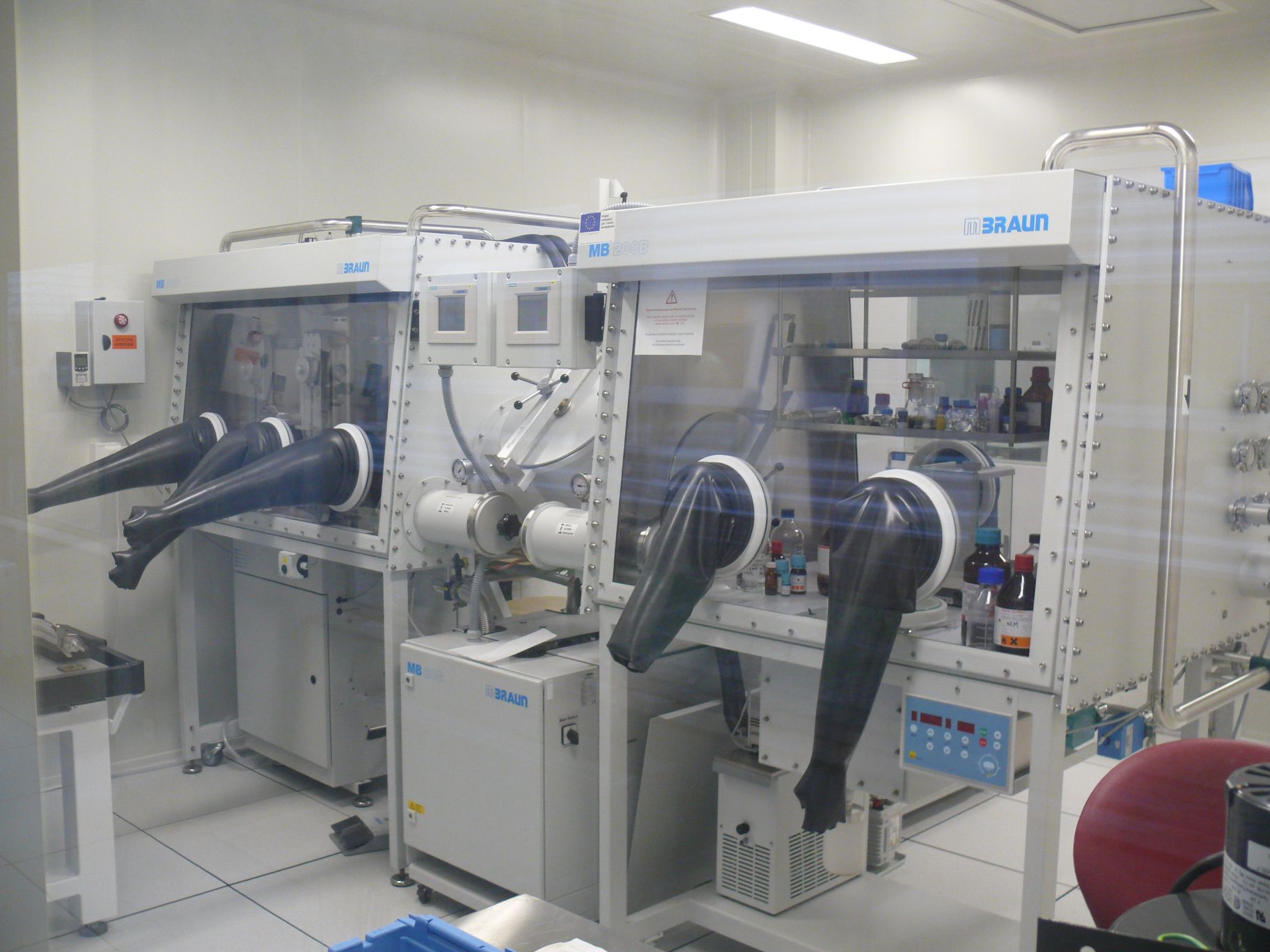
None of this is heading for a desktop resin printer anytime soon — two-photon nanoprinting systems are specialized, expensive, research-grade instruments meant for shared university core facilities like UCSB's Nanofab rather than an individual lab bench, a world away from the countertop SLA and FDM printers most hobbyists use. But the underlying story is one that matters to anyone following where additive manufacturing is headed as a field.
For years, the pitch for 3D printing at the macro scale has been "print things you couldn't machine." At the nanoscale, the pitch is the same, but the payoff is arguably bigger: photonic components, ion-trap electrodes, and cell scaffolds that are difficult to make with subtractive or planar-lithography techniques because those techniques are fundamentally limited to flat, stacked geometry. A university investing $1.15 million specifically to move past that limitation — buying equipment described by the researchers as producing structures "no longer constrained by geometry nor confined to two-dimensional planes" — is a signal that the frontier of additive manufacturing research is shifting from "how fine can we make each layer" to "how do we stop thinking in layers at all."
It's also worth noting how this grant was structured: one facility, five co-PIs, four research areas. That's a fairly common pattern for university core facilities funded through NSF instrumentation programs — rather than each lab buying its own limited equipment, a shared high-end tool gets acquired once and made available across departments. Coverage of the grant also notes plans for workforce-development ties through a regional micro/nanotechnology education partnership involving Santa Barbara City College and the California NanoSystems Institute, underscoring that the investment is meant to ripple outward rather than sit in one lab. For the broader 3D-printing ecosystem, this is where a lot of tomorrow's manufacturing techniques get incubated: a shared piece of nanofab equipment used by quantum physicists, biomedical engineers, and chemical engineers alike, each pushing it in different directions until something becomes robust enough, and cheap enough, to trickle down toward more accessible tools.
UCSB hasn't given a timeline for when the new nanoprinting system will be installed and operational in the Nanofab, nor specifics on the vendor or exact system model. Those details, along with the first published results from any of the four application areas, are the things worth watching for as this grant moves from funding announcement to working hardware.