Tungsten has a reputation among metallurgists that it has fully earned. It is the metal you want facing a fusion plasma, and it is also one of the worst metals to shape into anything. That is why a recent milestone matters. According to ANS Nuclear Newswire's Nov. 5 report, a team from North Carolina State University, Oak Ridge National Laboratory and JEOL used electron-beam powder bed fusion (EB-PBF) to print full-size tungsten tiles. The tiles were installed in the DIII-D tokamak and survived plasma exposure. According to VoxelMatters, the whole effort, from invitation to installation, took about eight months.
Fusion reactors will not be built from printed tiles anytime soon. Still, the result shows an additive process making parts at the size, in the material and under the conditions that plasma-facing hardware has to meet. The reasons it was difficult explain why the outcome is notable.
Why Tungsten Fights Back
The case for tungsten is simple. As VoxelMatters notes, it melts at 3,422 °C, the highest of any metal, so it can take heat loads that would erode most alternatives. The trouble starts once it cools. Tungsten has a ductile-to-brittle transition, and VoxelMatters says it cracks below roughly 200 to 600 °C. ANS makes the same point: that transition temperature, together with the very high melting point, makes tungsten hard to manufacture into the required shapes with traditional processes.
Laser powder bed fusion has not been a good fit. VoxelMatters reports that most laser-printed tungsten attempts have ended up porous and cracked. A crack running through a printed part is not something finishing can repair, which is why Michael Kirka of ORNL says most of the field thought printed tungsten would always crack.
EB-PBF gets around much of this. According to VoxelMatters, the beam holds the surrounding material above 1,400 °C during the build. That keeps the powder bed well above the ductile-to-brittle range, so the printed tungsten is not sitting in its brittle regime while the part is being built. ANS adds that this happens layer by layer in a vacuum chamber. According to NC State, as relayed by ANS, the university and ORNL used this method several years ago to produce dense, crack-free tungsten.
From Buttons to Tiles
This was not the team's first trip into a tokamak. ANS reports that in 2025 the collaborators tested small printed tungsten "buttons" using DIII-D's Divertor Materials Evaluation System. Those samples saw heat flux near 20 MW/m², with brief peaks above 35 MW/m², and showed minimal surface damage. After that result, the team was asked to test a full-size printed tile.
The 2026 tiles answer that question on size. Each tile measures about 140 x 130 mm, according to both sources. The largest tungsten print NC State had made before was about 50 mm across. According to Tim Horn of NC State's Center for Additive Manufacturing and Logistics, the university's own machines could not hold such a high-temperature material at the required conditions over a build that large.
So the work was split among the partners. JEOL, which has a large-format EB-PBF system, the JAM-5200EBM, and had been developing tungsten printing on its machines, printed several iterations of flat and domed designs at its facility in Akishima, Japan, and produced tiles that met design tolerances without major defects. NC State finished the parts with wire electrical discharge machining and CNC grinding, giving the plasma-facing surfaces mirror-like finishes. VoxelMatters adds that ORNL funded the fabrication. ANS's coverage includes comments from Kirka and Horn, and VoxelMatters also quotes Florian Laggner, an assistant professor of nuclear engineering at NC State, on the tokamak side of the project.
What Happened in the Tokamak
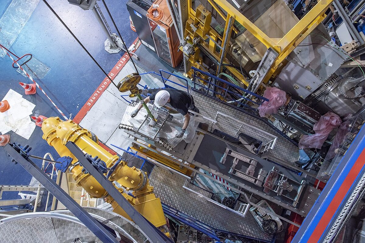
According to ANS, the tiles were mounted on copper-alloy pedestals and installed in DIII-D's lower divertor in July 2026. Over the Tile Testing Campaign they saw three days of direct plasma exposure, including 74 high-confinement "H-mode" discharges at medium-to-high power. Both sources say the tiles came through intact. VoxelMatters quotes Jonathan Coburn of Sandia National Laboratories, who led the campaign's novel tile testing: "As far as we could tell in the control room, your AM tiles performed really well."
That is a survival result, not a final verdict. ANS says the tiles are now being removed, imaged and surface-scanned to compare with their condition before exposure, with NC State leading the analysis.
Why the Finishing Step Matters
Anyone who has used a metal printer knows the as-built part is rarely the finished part, and these tiles are no exception. Wire EDM erodes material with electrical discharges instead of cutting it mechanically, which is why it is a common way to shape hard metals. CNC grinding then produced the mirror-like plasma-facing surfaces. The sources do not explain why those finishes matter thermally, but it is reasonable to infer that dimensional control is part of how a plasma-facing part performs, not a cosmetic step.
The Fusion Context
VoxelMatters gives a useful benchmark: future fusion power plants will need tiles that handle steady loads of 10 to 20 MW/m². The 2025 buttons saw about 20 MW/m² with brief peaks above 35 MW/m², which puts the printed material in a relevant range. Now that full-size tiles have also come through plasma exposure, the main questions move from "can it be printed?" to longer-term ones like lifetime, cycling and qualification. The sources do not claim those questions are settled.
The eight-month timeline is significant too. Going from invitation to installed hardware in under a year suggests that additive manufacturing could let fusion researchers test new part designs quickly, though two sources on one project are not proof of a general trend.
What It Means for Makers
To be clear up front: nobody is printing tungsten on a bench machine. EB-PBF requires a vacuum chamber, a high-power electron beam and enough budget that a JEOL JAM-5200EBM is not a hobby purchase. The lessons, though, apply to anyone who prints.
First, process temperature is a material property in practice. The tungsten itself is unchanged. What makes it printable is holding the surrounding material above 1,400 °C so it does not sit in its brittle range while the part is built. The same principle applies, at much lower temperatures, to the heated chambers that keep ABS, nylon and high-temperature engineering filaments from warping and delaminating. Control the thermal history and you control the defects.
Second, scaling up is a separate problem from proving the material. Moving from small buttons to tiles about 140 mm across, against a previous largest print of about 50 mm, took its own engineering effort and a different machine. Anyone who has watched a print that worked fine at 50 mm curl at the corners when scaled up will recognize that.
Third, printing is one step in a longer process. The tiles needed EDM and grinding before they were ready for the tokamak. Planning for post-processing from the start, with machining allowance, datum surfaces and fixturing, separates a nice print from a functional part at any scale.
Bottom Line
Electron-beam printing has made tungsten, a notoriously difficult material, into full-size parts that survived plasma inside a working tokamak, and the team did it in about eight months. It does not mean printed reactor walls are coming soon, but it is good evidence that AM can make hardware for fusion's harshest environment.