
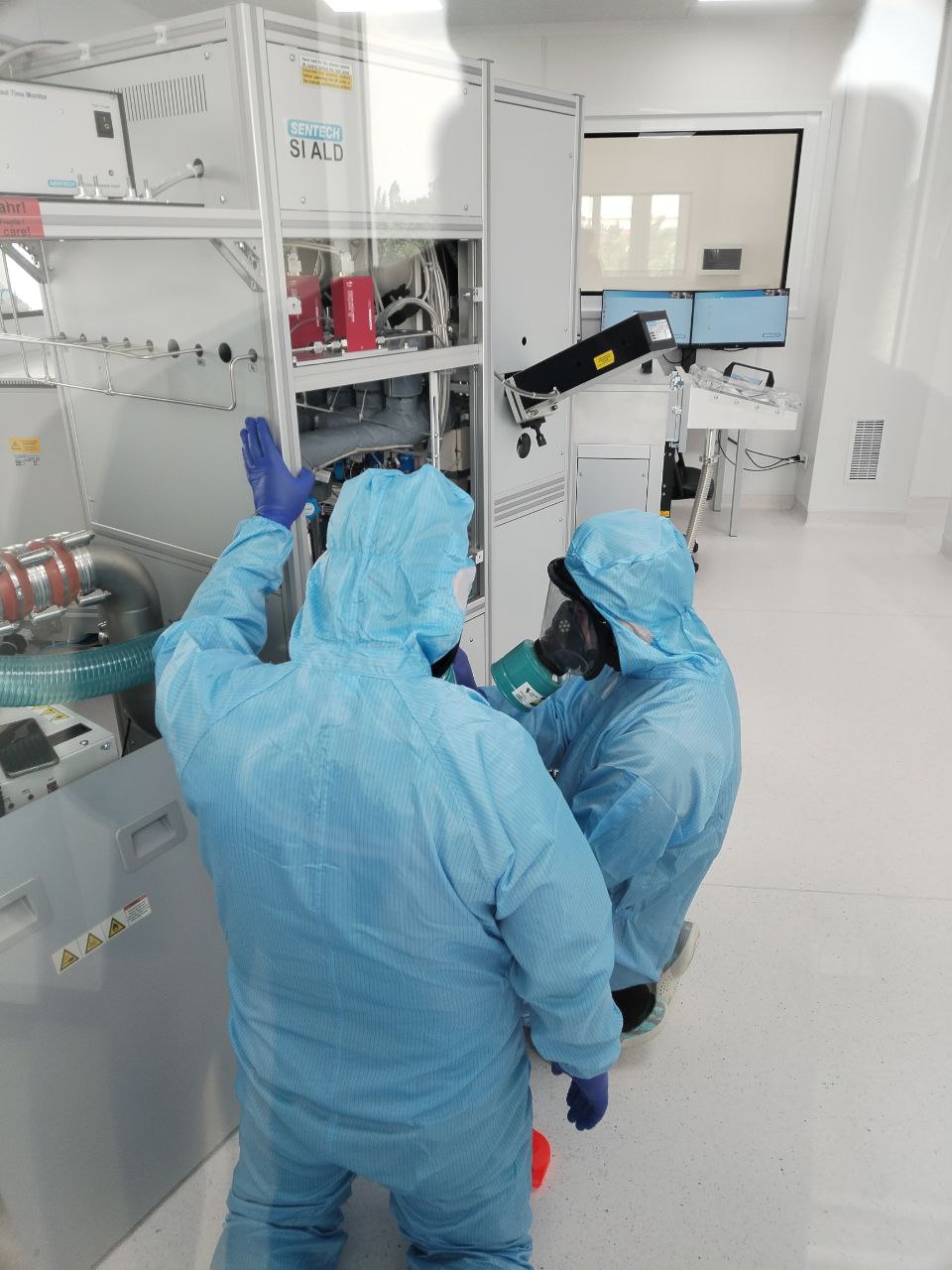
Most of what gets covered on this site involves melting plastic, sintering metal powder, or curing resin — processes measured in tenths of a millimeter. ATLANT 3D's newest machine operates at a scale about five orders of magnitude smaller. On August 17, 2026, the Danish company announced NANOFABRICATOR PRO, a system it describes as the "world's first and only physical platform for AI-driven materials discovery" — a printer that builds structures one atomic layer at a time and is meant to close the loop between an AI model's material predictions and an actual, physical sample sitting on a substrate.
If that sounds like it belongs in a semiconductor fab rather than a maker's workshop, that's roughly the point. NANOFABRICATOR PRO isn't a desktop machine for hobbyists — it's aimed at labs and production lines working in chip manufacturing, photonics, MEMS sensors, advanced packaging, and quantum devices. But the underlying idea — additive manufacturing guided by algorithmic design rather than trial-and-error — is one that's been creeping steadily down from industrial R&D into more accessible corners of the maker world, and it's worth understanding where the leading edge currently sits.
What Atomic Layer Printing Actually Means
The core technology is what ATLANT 3D calls Direct Atomic Layer Processing, or DALP — a proprietary evolution of atomic layer deposition (ALD), a technique long used in chip fabs to grow ultra-thin, ultra-uniform films by cycling reactive gas precursors across a surface one molecular layer at a time. Conventional ALD is a blanket process: it coats an entire wafer uniformly, and patterning has to happen separately through lithography and etching. DALP, according to the company, applies that atomic-scale precision directly and selectively, which is the difference between "coating everything" and "printing" in any meaningful sense of the word.
NANOFABRICATOR PRO is built on top of that process and serves as the physical foundation of ATLANT 3D's broader "A-HUB Autonomous Materials Foundry" concept — what the company, in its launch materials, calls "the foundation of the Physical AI Infrastructure for Matter." VoxelMatters describes the same concept as "linking digital materials discovery with physical experimentation to enable more autonomous materials innovation." In practice, that means an AI system proposes candidate materials or thin-film structures, the printer fabricates them at atomic precision, and the resulting devices are tested and fed back into the model — what ATLANT 3D CEO Dr. Maksym Plakhotnyuk described in the launch announcement as enabling "rapid translation of computational predictions into functional materials."
Built in the US, Aimed at Chips and Quantum Hardware
Despite being a Danish company headquartered in Taastrup, ATLANT 3D is having NANOFABRICATOR PRO manufactured in the United States by Automated Industrial Robotics (AIR), with the hardware built to SEMI compliance standards — the equipment specifications semiconductor fabs require for tools entering their production environments. That's a meaningful detail: it signals ATLANT 3D isn't positioning this as a lab curiosity but as something that could plausibly sit on a fab floor or in an industrial R&D pilot line without a redesign.
Trade outlet VoxelMatters, covering the launch on August 18, quoted both Plakhotnyuk and AIR President Bob Fung framing the collaboration around turning AI-discovered materials into working devices via hardware that's actually production-ready rather than a one-off prototype tool. Fung put it this way: "Our partnership combines advanced engineering with U.S. manufacturing capabilities to deliver the NANOFABRICATOR PRO platform to enable next frontiers for future industries." The pitch is squarely industrial: semiconductors, advanced packaging, and quantum technologies are the named target markets in ATLANT 3D's own announcement, while VoxelMatters' reporting broadens that list to microelectronics, photonics, MEMS, and packaging — applications consistent with the photonics and MEMS work ATLANT 3D has pursued with its DALP platform generally.
ATLANT 3D itself was founded in 2018 and has raised more than $30 million to date, including a $15 million Series A+ round led by West Hill Capital. Its customer and investor list already includes NASA, Sony, and STMicroelectronics — names that point toward a company selling into aerospace, consumer electronics, and semiconductor supply chains rather than the prosumer 3D printing market this site typically covers.
What It Means for Makers
Let's be direct: nobody reading this is putting a NANOFABRICATOR PRO next to their Bambu Lab or Prusa anytime soon. This is industrial capital equipment serving chip fabs and quantum-hardware labs, not a machine that will show up at a maker faire. But there are two reasons it's still worth makers' attention.
First, atomic layer deposition and its variants have a track record of eventually trickling into more accessible tools — much as SLA resin printing, once an industrial-only process, became a $200 desktop appliance within a decade. If DALP proves out commercially, the underlying selective-deposition concept could eventually inform lower-cost tools for makers doing serious electronics, sensor, or MEMS prototyping, even if a full atomic-precision system stays well out of reach for years.
Second, and more immediately relevant: the "AI proposes, printer fabricates, results validate the model" loop that ATLANT 3D is building into A-HUB is a pattern worth watching regardless of scale. Slicer software, print-farm orchestration, and generative design tools have all been absorbing AI-driven feedback loops over the past few years, and a company explicitly building "materials discovery" hardware around that workflow is a signal of where R&D-adjacent fabrication tooling is heading. Makers building anything with functional materials — conductive traces, custom filaments, composite formulations — are already doing crude versions of iterate-test-refine; watching how an atomic-scale system automates and accelerates that loop is a useful preview of tooling patterns that tend to migrate downmarket over time.
Bottom Line
NANOFABRICATOR PRO is a serious, SEMI-compliant industrial tool built for chip fabs, photonics labs, and quantum-hardware developers — not a printer for makers' benches. Its news value here is less about the specific hardware and more about the trend it represents: additive manufacturing pushed to the atomic scale and wired directly into an AI discovery loop, with a well-funded company (backed by NASA, Sony, and STMicroelectronics as customers) betting that closing that loop physically, not just in simulation, is the next unlock for materials R&D. Whether or not any of that hardware ever reaches a price point makers can touch, the workflow pattern it's built around is worth keeping an eye on.
